
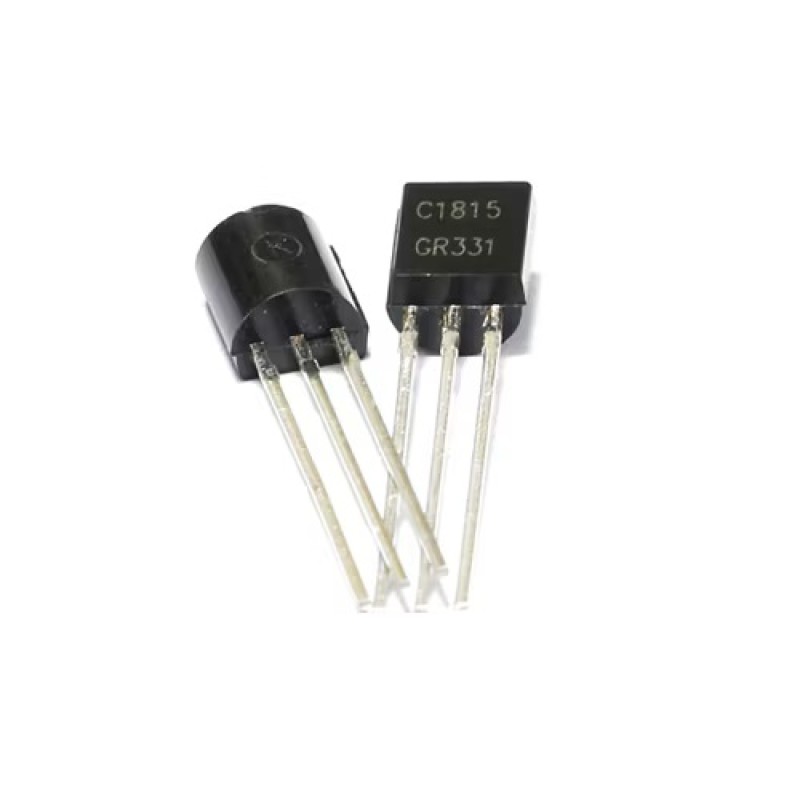
The C1815 transistor is a fundamental component in a wide range of electronic circuits, playing a crucial role in modern electronics. As a general-purpose NPN transistor, it is particularly well-suited for low-noise applications, making it an excellent choice for audio frequency amplification and switching circuits. With its high gain, low power consumption, and affordability, the C1815 has become a popular option for engineers, electronics enthusiasts, and DIY hobbyists. Whether used in small-signal amplification, switching operations, or digital logic circuits, this versatile transistor continues to be a reliable and efficient solution for various electronic applications.
What Is the C1815 Transistor?
The C1815 is an NPN bipolar junction transistor (BJT) widely used for switching and signal amplification in various electronic circuits. As a three-terminal device, it regulates current flow between the collector and emitter, with the base current serving as the control input. This fundamental characteristic allows it to function effectively as both a signal amplifier and an electronic switch.
Due to its low noise performance, high gain (hFE), and fast switching capability, the C1815 transistor is widely employed in audio amplifiers, radio frequency circuits, digital logic applications, and signal processing systems. Its compact TO-92 package, low power consumption, and affordable cost further contribute to its popularity among engineers, students, and electronics hobbyists. Whether used in consumer electronics, communication devices, or DIY projects, the C1815 remains an essential component in modern circuit design.
Key Specifications of the C1815 Transistor
The C1815 is a versatile NPN bipolar junction transistor (BJT) designed for low-power amplification and switching applications. Below are its key specifications:
1. Electrical Characteristics
-
Maximum Collector-Emitter Voltage (VCE): 50V – The highest voltage that can be applied between the collector and emitter.
-
Maximum Collector-Base Voltage (VCB): 60V – The maximum voltage allowed between the collector and base.
-
Maximum Emitter-Base Voltage (VEB): 5V – The highest voltage that can be applied between the emitter and base.
-
Maximum Collector Current (IC): 150mA – The maximum current that can flow through the collector.
-
Power Dissipation (PD): 400mW – The total power the transistor can safely handle without overheating.
2. Gain and Frequency Response
-
DC Current Gain (hFE): Typically ranges from 70 to 700, depending on the operating conditions. This indicates how well the transistor amplifies the input current.
-
Transition Frequency (fT): 80MHz – The frequency at which the current gain drops to 1, making it suitable for high-frequency applications.
3. Input and Output Impedance
-
Input Impedance: The transistor's base has relatively high impedance, which helps minimize loading effects in circuits.
-
Output Impedance: The collector has a lower impedance, making it effective in driving subsequent circuit stages.
4. Package Type and Dimensions
-
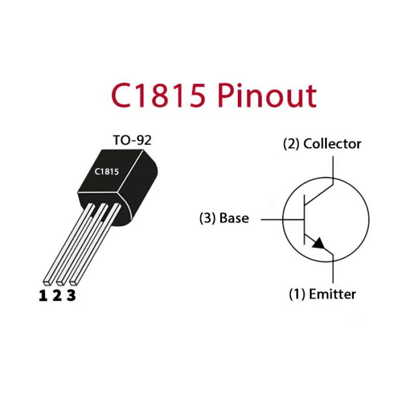
Package: TO-92 – A small plastic-encased package commonly used for low-power transistors.
-
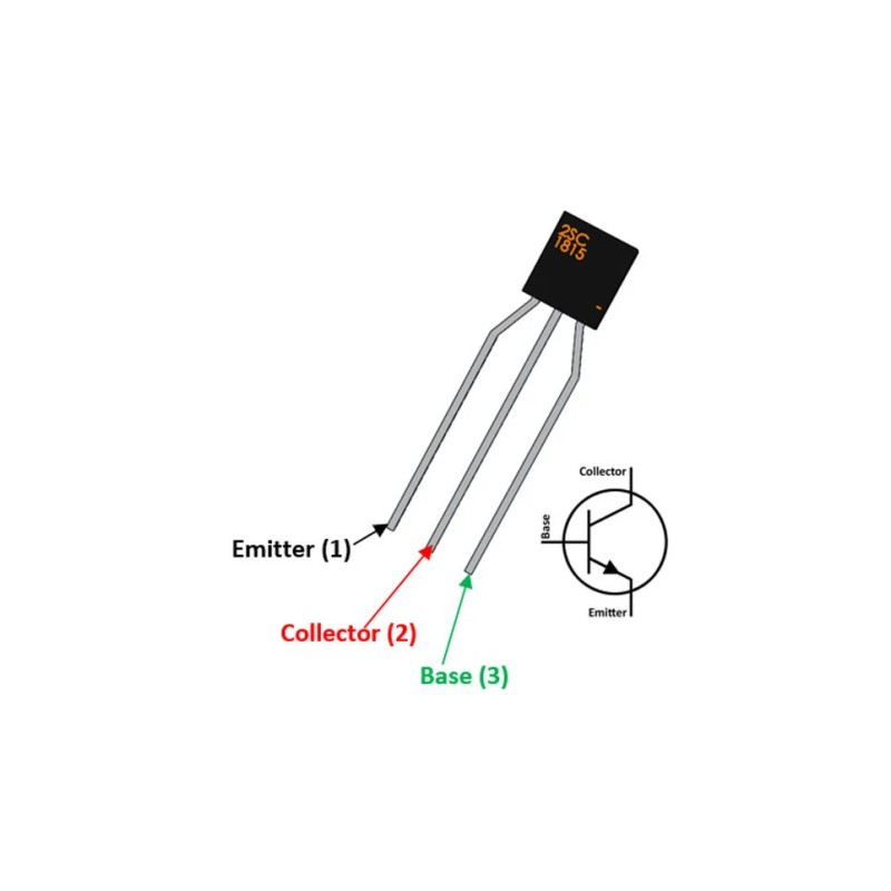
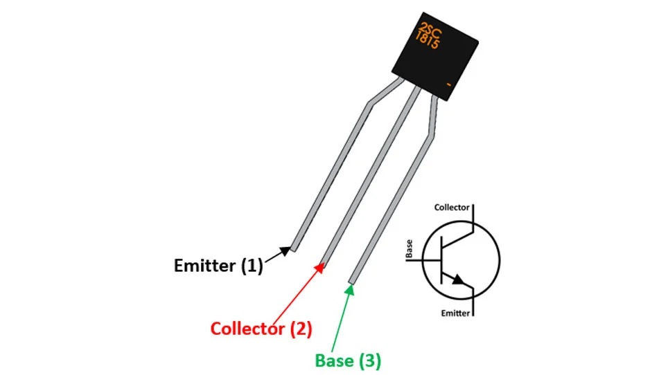
Pin Configuration:
-
1: Emitter (E) – The current exits the transistor.
-
2: Collector (C) – The main current flows through this terminal.
-
3: Base (B) – The control terminal that regulates the transistor’s operation.
-
-
Size: Compact and lightweight, making it ideal for space-constrained circuit boards.
Why These Specifications Matter
The C1815 transistor’s combination of low noise, high gain, and fast switching makes it particularly suitable for audio amplification, signal processing, and low-power switching applications. Its moderate voltage and current ratings also make it a reliable choice for general-purpose electronic projects.
4. Pinout Configuration of the C1815
The C1815 transistor follows a standard TO-92 package pinout, consisting of three terminals: Base (B), Collector (C), and Emitter (E). Each pin plays a crucial role in the transistor’s functionality.
Pin Descriptions
-
Base (B) – The control terminal that regulates the transistor's operation. A small current at the base allows a much larger current to flow from the collector to the emitter.
-
Collector (C) – The output terminal where the main current flows. It connects to the positive voltage supply in most circuit applications.
-
Emitter (E) – The current return path. It is typically connected to the ground or negative voltage supply in a circuit.
TO-92 Package Pinout Layout
When viewing the transistor from the flat side with the leads facing downward, the pin configuration is as follows:
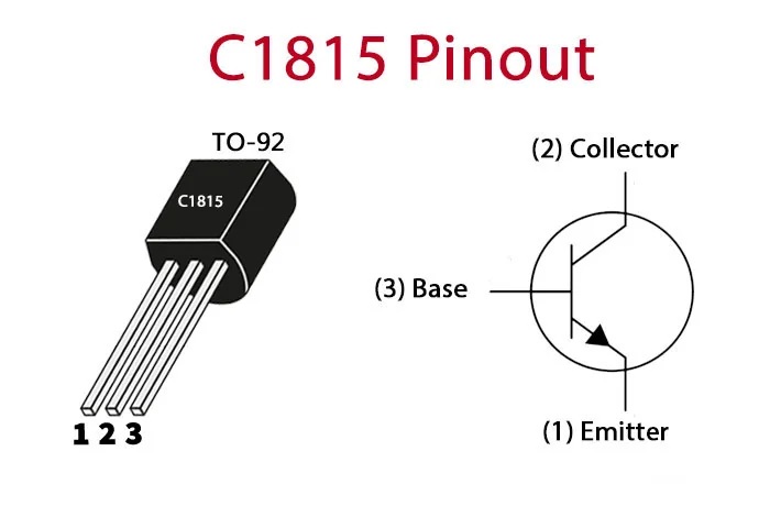
(Left to Right: Emitter – Collector – Base)
Pin Functionality in Different Circuit Applications
-
As a Switch: The base receives a small current to control a larger current flow between the collector and emitter, turning a connected circuit on or off.
-
As an Amplifier: The transistor amplifies small input signals at the base, producing a larger output signal at the collector.