


Dual MC33926 Motor Driver Carrier
 לחץ להגדיל |
|
Dual MC33926 Motor Driver Carrier
This dual brushed DC motor driver, based on Freescale’s MC33926 full H-bridge,
has a wide operating range of 5 – 28 V and can deliver almost 3 A continuously (5 A peak) to each of its two motor channels.
The MC33926 works with 3 – 5 V logic levels, supports ultrasonic (up to 20 kHz) PWM,
and features current feedback, under-voltage protection, over-current protection, and over-temperature protection.
The dual MC33926 motor driver carrier is a breakout board featuring two Freescale MC33926 H-bridge ICs.
It can supply up to almost 3 A continuous current per channel to two brushed DC motors
at 5 – 28 V, and it can tolerate peak currents up to 5 A per channel for a few seconds,
making this a great general-purpose motor driver for medium-sized DC motors and for differential-drive robots that use such motors.
The MC33926 supports ultrasonic (up to 20 kHz) pulse width modulation
(PWM) of the motor output voltage, which eliminates the audible
switching sounds caused by PWM speed control, and a current feedback circuit for each motor outputs an analog
voltage on its respective FB pin that is proportional to the output current.
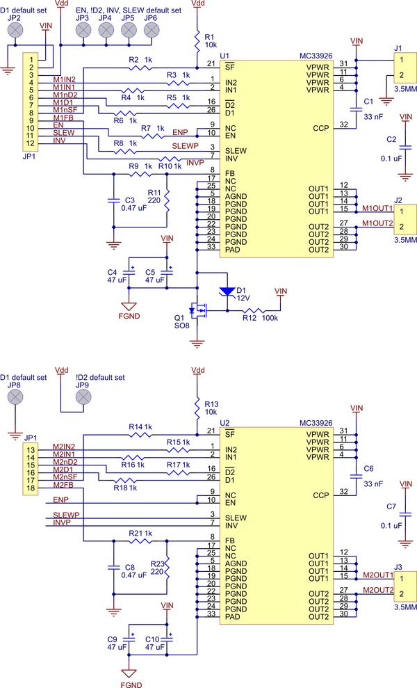
Since this board is a carrier for the Freescale Semiconductor MC33926 H-bridge,
we recommend careful reading of the MC33926 datasheet (1MB pdf).
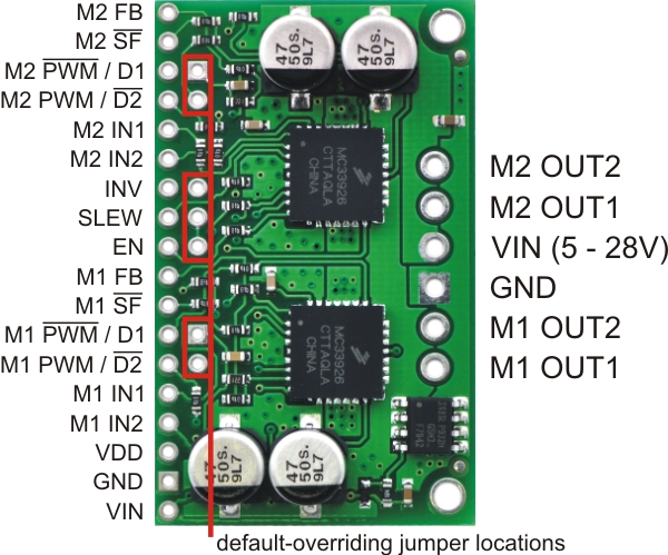
The default states of many of the MC33926 logic input pins requires that many external connections be made to use this board.
To reduce the number of necessary external connections, the board has seven default-overriding jumpers.
All of the default-overriding jumpers are tied to VDD, except the D1 jumpers,
which are tied to GND. All VDD jumper pads are circles; the ground jumper pads are square.
Note that the board has only one invert, slew, and enable pin; each of these three pins affects both motor drivers.
| PIN | Default State | Description |
|---|---|---|
| VIN | HIGH | This is the main 5 – 28 V motor power supply connection, which should typically be made to the larger VIN pad. Operation from 5 – 8 V reduces maximum current output; the device is also protected for transients up to 40 V. The smaller VIN pad can be used to distribute the VIN node to the rest of the application circuit; for lower-current applications, the pin can also be used to power the board and motors. |
| GND | LOW | Ground connection for logic and motor power supplies. |
| OUT2 | HIGH | The motor output pin controlled by IN2. |
| OUT1 | HIGH | The motor output pin controlled by IN1. |
| VDD | HIGH | 3-5 V logic supply connection. This pin is used only for the SF pull-up and default-overriding jumpers; in the rare case where none of those features is used, VDD can be left disconnected. |
| IN2 | HIGH | The logic input control of OUT2. PWM can be applied to this pin (typically done with both disable lines inactive). |
| IN1 | HIGH | The logic input control of OUT1. PWM can be applied to this pin (typically done with both disable lines inactive). |
| PWM / D2 | LOW | Inverted disable input: when D2 is low, OUT1 and OUT2 are set to high impedance. A D2 PWM duty cycle of 70% gives a motor duty cycle of 70%. Typically, only one of the two disable pins is used, but the default is for both disable pins to be active. |
| PWM / D1 | HIGH | Disable input: when D1 is high, OUT1 and OUT2 are set to high impedance. A D1 PWM duty cycle of 70% gives a motor duty cycle of 30%. Typically, only one of the two disable pins is used, but the default is for both disable pins to be active. |
| SF | HIGH | Status flag output: an over-current (short circuit) or over-temperature event will cause SF to be latched LOW. If either of the disable pins (D1 or D2) are disabling the outputs, SF will also be LOW. Otherwise, this pin is weakly pulled high. This allows the two SF pins on the board to be tied together and connected to a single MCU input. |
| FB | LOW | The FB output provides analog current-sense feedback of approximately 525 mV per amp. |
| EN | LOW | Enable input: when EN is LOW, the both motor driver ICs are in a low-current sleep mode. |
| SLEW | LOW | Output slew rate selection input. A logical LOW results in a slow output rise time (1.5 μs – 6 μs). A logical HIGH selects a fast output rise time (0.2 μs – 1.45 μs). This pin should be set HIGH for high-frequency (over 10 kHz) PWM. This pin determines the slew rate mode for both motor driver ICs. |
| INV | LOW | A logical high value inverts the meaning of IN1 and IN2 for both motor drivers. |
ביקורת : הערה ללא תרגום מ HTML!
דירוג רע טוב
הכנס את הקוד התיבה

לחץ להגדיל
לחץ להגדיל

לחץ להגדיל

לחץ להגדיל

לחץ להגדיל
